Practical Methods for Decapping Chips
Most, if not all, of the devices that we employ in our digital lives have a physical presence within our homes and workplaces. Beyond just the laptops we use every day, many of us have devices all around us, perhaps packed away on a shelf or hidden from direct view in the form of some little plastic doodad, that interact with either each other or the internet. While all of these digital devices may seem worlds apart, if you were to take any of them apart, eventually you will encounter their printed circuit boards (PCBs) underneath. While these boards may seem simple, they contain the complex circuitry that enables their functionality. At the heart of these PCBs are integrated circuits (ICs), which are tiny silicon chips – also known as die’s. These are cut from a larger wafer, which contain many copies of the design in a grid that perform specific tasks.
Typically, the inner workings of these chips are hidden from view, encapsulated in protective epoxy. However, for those curious about the underlying technology, a process known as decapsulation, or “decapping” can reveal these secrets. By carefully removing the protective casing, we can access the chip’s die, the tiny piece of silicon that contains the actual circuitry.
This blog post will guide you through methods of chip decapping that are practical for home or amateur lab settings. These methods are designed for situations where the equipment and expertise required to handle acids are not available, making them accessible for hobbyists and enthusiasts. Our goal is to democratize safe access to reverse engineering capabilities that are typically considered out of reach for anyone without a well-funded reverse engineering laboratory. Modern ICs with smaller or more complex process nodes often require more precise decapping techniques, due to considerations which we will cover in a future blog post. For now, this post focuses on approachable methods, highlighting considerations for choosing the best techniques for commonly encountered semiconductor fabrication methods and packaging types, and the eventual imaging requirements.
Let’s explore how to uncover the secrets of silicon in a safe and practical manner, and expose them to the light of day.
Why bother decapping?
Below is a simplified diagram of how chips are assembled. The die is the area of the chip we are interested in accessing.

When you peer into the heart of a de-capped chip, you’ll discover a miniature world of intricate circuitry. The die, a tiny silicon chip, seen labeled above, is the heart of the device. It is here that the magic happens, where millions of transistors perform complex calculations and process information. If you look closely, you can see the die, the bonding wires, the architecture inside the die, how it is laid out, what structures are used, where memory is kept, and, in some cases, watermark and manufacturer information stamped into the die.
This can be an extremely rewarding endeavor. However, this process is fraught with risks. A misstep can lead to the destruction of the die or damage to the delicate bonding wires. Contamination from dust or other particles can also compromise the integrity of the chip.
NOTE: Decapping is considered an invasive to semi-invasive technique, and therefore seen as risky, as the chip or PCB functions may not survive. Always use proper protection, safety glasses, ventilation, etc., and do not decap anything you cannot afford to lose.
The Classic Method: Acid
When we think of chip decapping, images of dangerous chemicals and intricate procedures often come to mind. It is a process that requires precision, patience, and a certain level of technical expertise.
The idea of slowly, methodically dissolving away layers of protective epoxy with harsh acids might seem daunting, and rightly so. It is a delicate operation that can easily go wrong. But the rewards can be significant, offering a glimpse into the inner workings of modern technology. Below are some examples of chips that have been successfully decapped with acid.
A misstep with acid can easily result in corrosion of the bonding wires. Contamination from dust or other particles can also compromise the integrity of the chip.
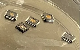

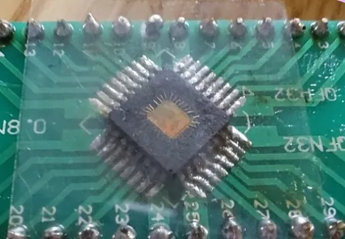
Acid etching is a crucial step in the normal decapping process, but it is also a highly dangerous one. It involves the use of a combination of strong acids such as nitric, sulfuric, hydrochloric, etc., all of which can cause severe burns and damage to organic tissue (you!) and property if not handled correctly.
As mentioned earlier, due to the inherent risks involved, we will not be providing detailed instructions or recommendations on acid etching in this blog post. There are many other resources available online and in print that offer comprehensive guidance on safe acid handling and etching techniques, for example https://jcjc-dev.com/2020/10/20/learning-to-decap-ics/.
Though if you do choose to work with acids it is essential to prioritize safety. Always wear appropriate protective gear, such as gloves, goggles, and a lab coat. Work in a well-ventilated area and be prepared to handle any potential spills or accidents. And research the proper methods of disposal, you do not want to pour these chemicals down the drain or out in your backyard as they could depending on the chemical combination, cause serious property damage or further safety hazards.
If you are unsure about any aspect of acid etching, it is best to consult with an experienced professional or seek additional information from reputable sources.
While using acid is the most common method for decapping, there are other methods that can be done with somewhat less risk and may be more accessible to hobbyists and researchers with limited resources. These techniques, discussed below, may work better in a small lab or home lab while still yielding favorable results.
The Simple Method: Heat and Brute Force
One of the simplest methods to expose a die for microscopic examination is to apply heat to the chip and then break the epoxy around it. While the chip will not be functional afterward due to the damage to its leads and frame, forensic analysis can still be conducted by examining it under a microscope. Depending on the extent of damage, the chip may even be reworked.
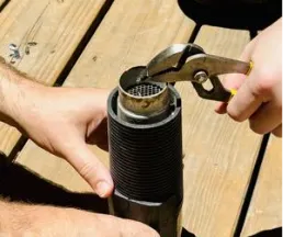
In this case, we use a heat gun normally used to strip paint as our heat source and use that to weaken the epoxy housing the chip. Epoxy tends to weaken around 250 to 500 degrees Fahrenheit. This is no problem for the pictured heat gun, which tops out at around 800 degrees.
Under this heat there is a slight discoloration, and the epoxy becomes much more brittle. The die can be removed with a little bit of force to peel the epoxy off of the die.

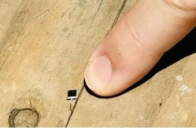
Once exposed, the die comes free of the epoxy, but so do all of the bonding wires, rendering it inoperable.
Still, you can see minute details of the chips. It can still be useful for reverse engineering in or identification of potential supply chain attacks.

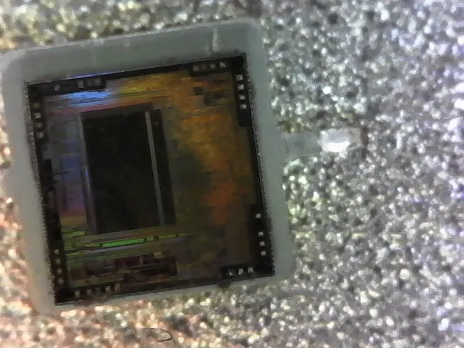
Chips decapped this way remind me of the LCARS user interface from Star Trek, I do not know why….
Here you can see some of the structures under the microscope. There is some debris still on the die from the decapping, but the layout of the chip is visible.
The Better Method: Sandpaper, Grinding, and Luck
If you need to decap the chip while keeping it functional and want to avoid exposure to acids or toxic fumes, another approach involves removing the underside of the chip rather than its surface. During manufacturing, dies are typically placed on a frame with external components (legs) attached, and these legs are connected to the die using wires (gold/aluminum, etc.) on the top side. By accessing the underside, you can often remove the metal plate using nothing more than a grinder and a bit of force.
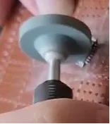
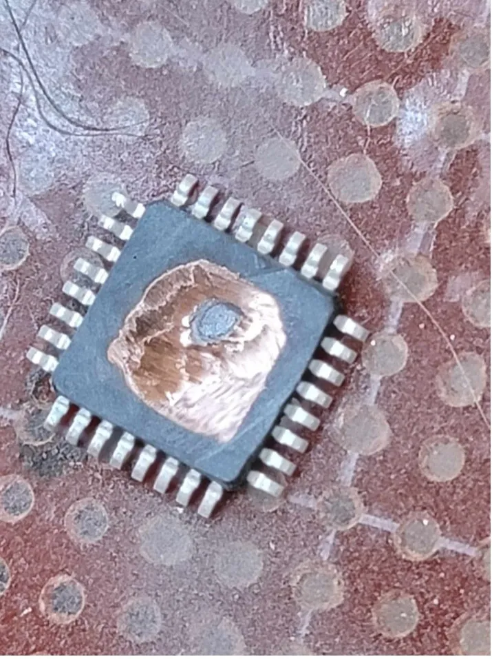
Note that even if you accidentally go too far, such as below, the chip may still function. Silicon on the bottom can often be abraded to thin the chip for imaging purposes, but the roughness of this surface will make it difficult to see properly, without lapping to a smoother finish.
Another approach is to stop grinding at the point pictured below, where you can see the base plate and the leads holding it to the package, but have not ground through the copper plate.
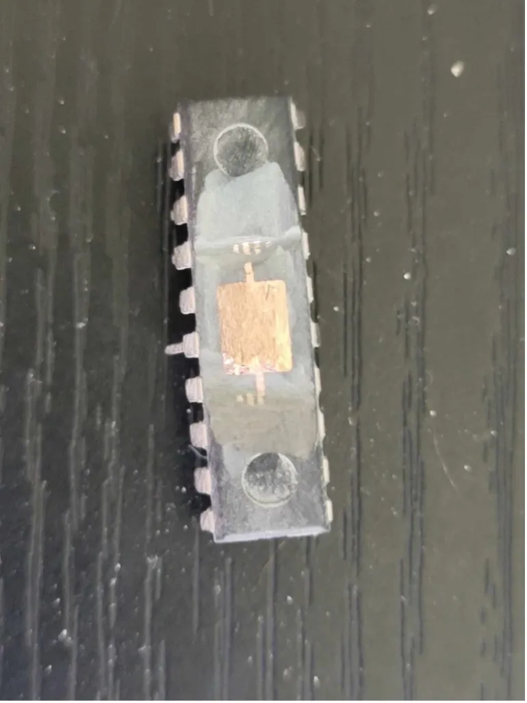
Here are three effective ways to remove the base plate:
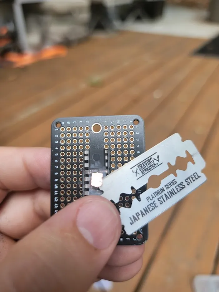
If you grind enough at one end, you will find that you can, with some effort, place a sharp instrument such as a safety razor blade between the copper and the epoxy. You are not trying to “lift” the copper, just separate the copper from the silicon and epoxy.
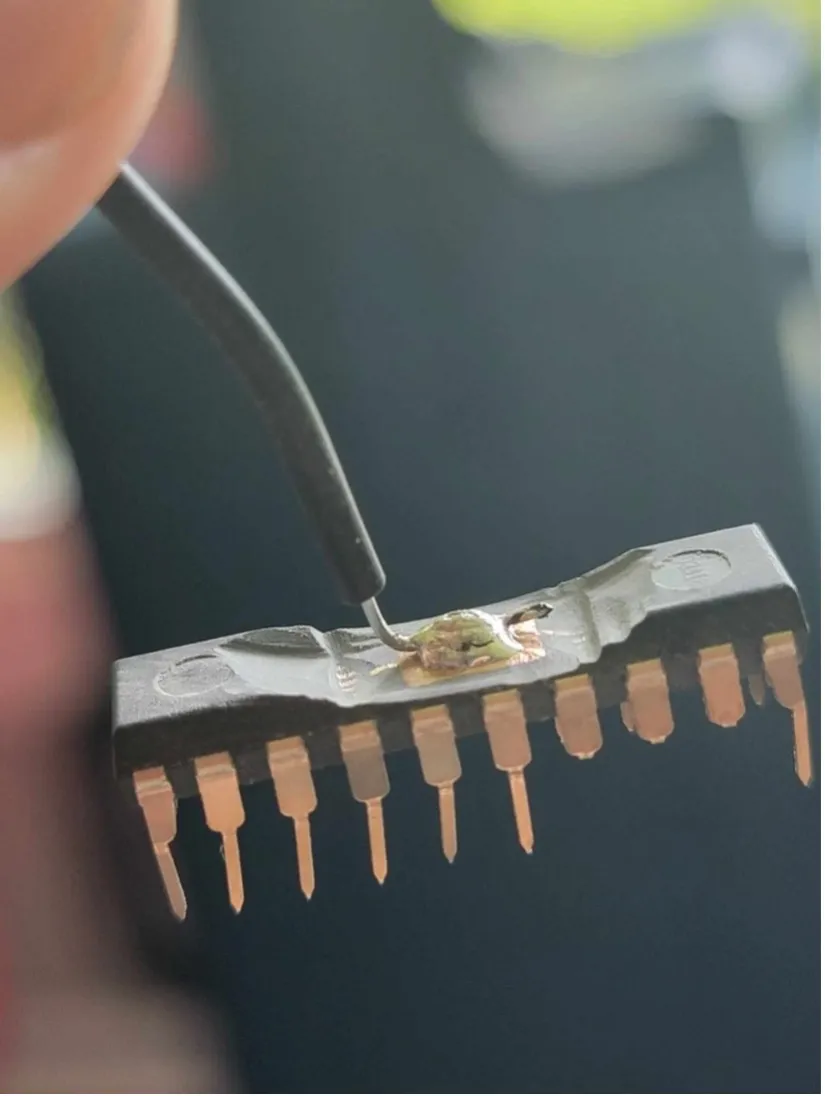
Use a lever. Below you can see that a stiff wire has been soldered to the base plate. By pulling on the wire in an even manner, you can cause the copper to separate like the opening of a book.
Throw caution to the wind and use power tools. Below is a belt sander being used to remove the back of a few chips for a talk at a conference. Sitting on the Belt sander is a ZIF (Zero Insertion Force) socket acting as an impromptu sanding block. We bent the pins 180 degrees and inserted the chip (now upside down) into the ZIF socket and removed the bottom layer of epoxy.


Once removed we are left with the following, still working devices with the bottom plate removed and the silicon die almost exposed. All that is left is a bit of thermal compound and epoxy keeping us from viewing the silicon.
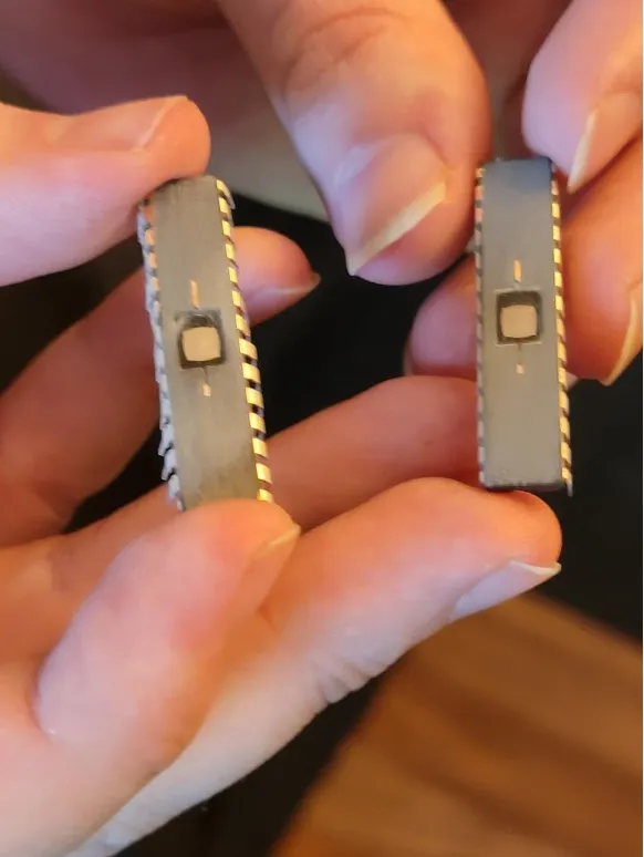
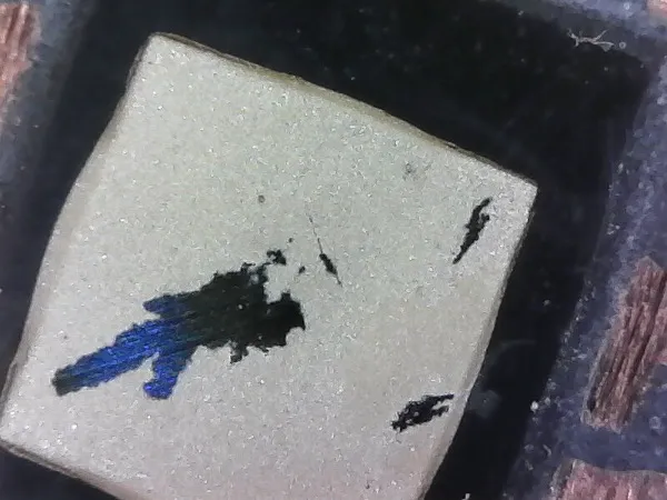
This grey glob of epoxy/thermal compound can be removed with some acetone and a soft plastic scraper, such as a guitar pick.
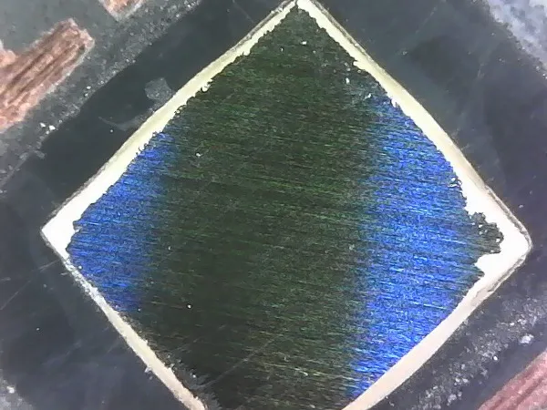
After some scraping the die is much clearer.
Once free of gunk, you will notice that the image is not as detailed as the with the heat method. The reason is that we are viewing the underside of the die and silicon is opaque to visible light (light we can see with our eyes). To see the circuitry on the front side of this chip, you will need a Near Infrared (NIR) camera capable of recording light with a wavelength around 1064 nm. Luckily, the Raspberry Pi NoIR V2 can see this wavelength, even though it exceeds the advertised range. When we designed the RayV-lite system, we used this camera and a 1064 nm light source to see into the chip. Please observe how this was done below.
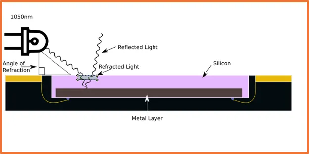
Below is a real-life example. The LED is placed at a 90-degree angle to the chip, and the integrated lens produces useful glancing illumination at an area around 30% from the base. This provides the correct angles to allow us to view the refracted light from inside the chip.
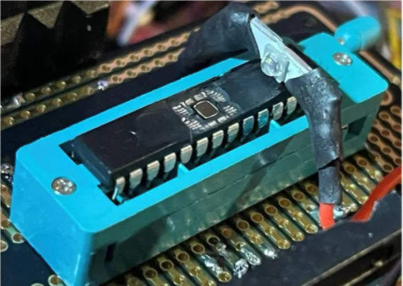
The following images were taken from the bottom side of the chip using this method with the RayV-lite microscope as referred to before.

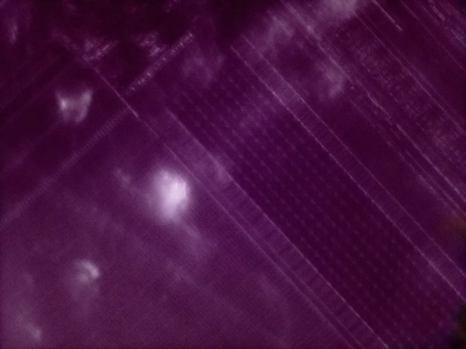
Now that you can see the internals of the chip, you can verify that it is the desired chip, and you can also perform experiments on the chip such as fault injection or side-channel analysis.
As technology continues to advance, so too will the techniques and tools attacking this technology. It is crucial that security researchers and enthusiasts are not limited by techniques that are dangerous or prohibitively expensive. By promoting safer and more accessible techniques like mechanical decapping, new researchers will have the ability to learn on these devices and come up with new methods of protecting them.
Explore more blog posts
Hijacking Azure Machine Learning Notebooks (via Storage Accounts)
Abusing Storage Account Permissions to attack Azure Machine Learning notebooks

Celebrating NetSPI’s Partners of the Year 2024
Congratulations to NetSPI’s 2024 Partner of the Year Recipients Defy Security, VLCM, Softcat, Enduir, Evotek, and AWS

Exploiting Second Order SQL Injection with Stored Procedures
Learn how to detect and exploit second-order SQL injection vulnerabilities using Out-of-Band (OOB) techniques, including leveraging DNS requests for data extraction.


